

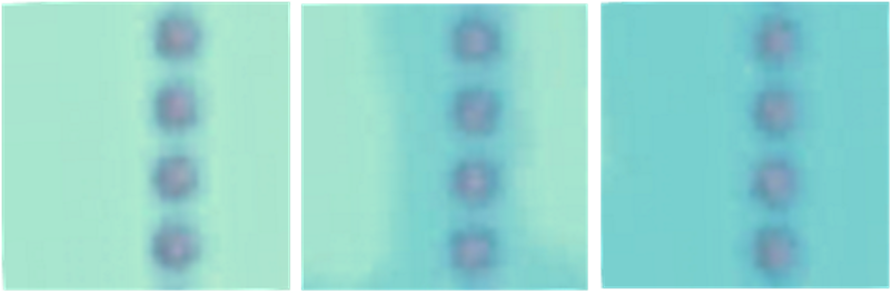
Custom layering. A single layer of the topological insulator WTe2 (green) was placed on top of a row of palladium seeds (each roughly 0.5 µm wide). Over time, palladium atoms spread out across the layer and formed Pd7WTe2 (blue-green). The sample is shown before heating (left), after 25 minutes at 210 °C (center), and after 65 minutes at 210 °C (right).
The researchers have now confirmed that this new material is superconducting. What’s more, they have explored other materials and have shown that the atom-spreading technique can work with a variety of ingredients. Of special interest is molybdenum ditelluride (MoTe2), as recent experiments showed that a twisted MoTe2 bilayer—a pair of single layers with one slightly rotated with respect to the other—exhibits a rare topological behavior called the fractional quantum anomalous Hall effect [3]. MoTe2 degrades in air, making its integration with other materials very challenging. Using a palladium seed, Wu and his colleagues were able to induce superconductivity in a twisted MoTe2 bilayer that was protected by layers of boron nitride above and below.
The researchers say that their technique offers a highly customizable method of introducing superconductivity into 2D topological materials. The atom spreading can be controlled to form superconducting disks or rings of desired sizes, and the resulting “islands” can be connected with bridges to form devices, such as circuit elements called Josephson junctions that are used in superconducting qubits. “With this technique, we can think of a 2D material as a canvas that we can ‘paint’ devices onto,” says graduate student team member Yanyu Jia. These devices could then be used to explore the properties of the superconducting state, potentially revealing the exotic behavior expected in topological superconductors.
Nanotechnology expert Christian Schönenberger from the University of Basel, Switzerland, says the new work is not fundamentally different from his own team’s recent demonstration of induced superconductivity in WTe2 [4]. But Wu believes that there are key differences between the two experiments, in particular, the larger area coverage that his team observes suggests a new mechanism for the movement of atoms. Materials scientist Yoichi Ando from the University of Cologne, Germany, agrees that a new—and surprising—chemical process seems to be at work. “I think this technique will be of interest to a broad range of researchers working on 2D materials as a new fabrication tool,” Ando says.
“This is a very exciting result,” says Xiaodong Xu from the University of Washington, Seattle, whose team observed the fractional quantum anomalous Hall effect in MoTe2 [3]. He says the new technique promises on-demand fabrication of 2D superconductors. “I can envision many new device structures enabled by this powerful approach,” Xu says. “In fact, my group has already reproduced some of these results after we learned of the work.”
References
- Y. Jia et al., “Superconductivity from on-chip metallization on 2D topological chalcogenides,” Phys. Rev. X 14, 021051 (2024).
- Y. Jia et al., “Surface-confined two-dimensional mass transport and crystal growth on monolayer materials,” Nat. Synth. 3, 386 (2023).
- H. Park et al., “Observation of fractionally quantized anomalous Hall effect,” Nature 622, 74 (2023).
- M. Endres et al., “Transparent Josephson junctions in higher-order topological insulator WTe2 via Pd diffusion,” Phys. Rev. Mater. 6 (2022).
Lead Image: Super spreading. A new technique for creating a superconducting layer involves placing a “seed” of metal (purple) on a 2D material (blue). When heated to around 200 °C, metal atoms spill out and spread over the surface. The resulting crystal is superconducting. Credit:
Y. Jia/Princeton University


